A Long-Sought Breakthrough in Solar Durability
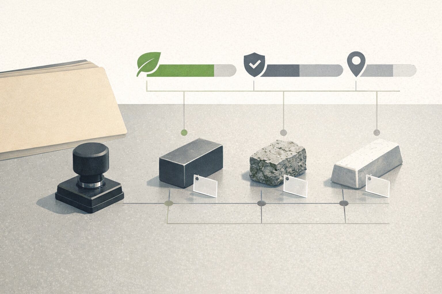
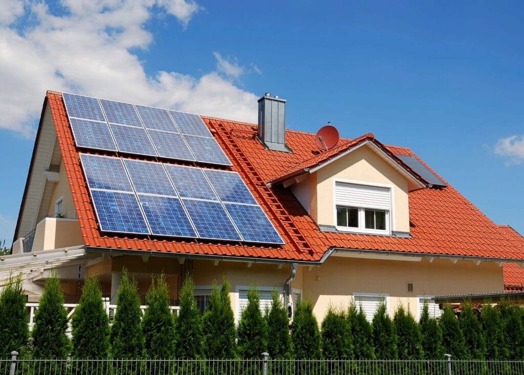
Perovskite solar cells have long been touted as the “next big thing” in solar energy. These cells use a special crystal structure (perovskite) that can be made from abundant materials and promise high efficiency at low cost. Until now, however, they’ve had one glaring Achilles’ heel: they just didn’t last long enough. Even as lab prototypes achieved over 25% efficiency, their power output would fade too quickly to survive 20-30 years on a rooftop. This month, that narrative changed. In early May 2025, researchers led by the University of Toledo and the National Renewable Energy Laboratory (NREL) announced a breakthrough solution – adding a simple ionic salt layer – that dramatically boosts perovskite solar cell durability. By swapping out a problematic carbon-based component (the C₆₀ layer commonly used in these cells) for a new salt-derived interlayer, the team tripled the mechanical toughness at a critical interface inside the cell. In practical terms, this means a much more robust solar cell, one that can maintain high performance for far longer than previous designs.
This development tackles the very stability issues that have kept perovskite photovoltaics (PVs) stuck in the lab. In tests, the new design hit 26% power conversion efficiency with only ~2% degradation after 2,100 hours of continuous operation at 65 °C. For context, that’s about three months of constant midday sunlight at a temperature hotter than a summer day in Arizona – with almost no loss in performance. Even when pushed harder (85 °C), the cells only lost ~5% after 1,500 hours. Scaled-up mini-modules (about 6 cm²) performed impressively too, achieving ~23% efficiency and under 9% degradation after 2,200 hours at 55 °C. Those numbers are among the best ever reported for perovskites and are on par with the early testing of today’s silicon panels. In short, a key technical barrier – long-term stability – is finally being overcome. And the fix was delightfully counterintuitive: replacing a fancy carbon molecule (buckminsterfullerene, or C₆₀) with a custom salt compound (dubbed “CPMAC”) that bonds more strongly and protects the cell’s sensitive layers. It’s a bit like discovering that sprinkling a pinch of salt can reinforce the glue holding your solar cell together.
For U.S. solar innovators and policy makers, this breakthrough could mark a turning point. Perovskite solar technology has been one of the few areas where American labs lead in intellectual know-how, yet commercialization has lagged due to durability concerns. Now that researchers have dramatically toughened up the cells’ endurance, the door is open for scaling up manufacturing. The question is: Will the U.S. seize this moment to build a homegrown solar manufacturing renaissance?
Why Tougher Perovskite Cells Change the Game
To appreciate why this advance matters, it helps to recall what makes perovskite cells so special – and so frustrating. Traditional silicon solar panels have dominated for decades; they’re reliable but have essentially hit an efficiency plateau around 22%. Perovskites, by contrast, are lightweight thin films that can be printed or coated onto surfaces, potentially much cheaper to produce. In just over ten years of R&D, perovskite cells catapulted from ~3% efficiency to over 25%, even rivaling silicon when used on their own. And in tandem configurations (a perovskite layer on top of a silicon cell), they’ve already surpassed 30% efficiency in the lab. The catch has been that perovskite cells were notoriously short-lived – prone to degrading from heat, moisture, UV light, and even internal reactions. One weak link was the interface between the perovskite layer and the electron transport layer (ETL) in the cell. In many perovskite designs (especially “inverted” cell architectures), a molecule called C₆₀ (a soccer-ball shaped carbon molecule) was used in that ETL. It helped shuttle electrons, but its molecular structure didn’t bond tightly, leading to a “weak interface” that eventually caused electronic and mechanical breakdowns. Think of it like a poor adhesive layer that starts to peel under stress.
The new ionic salt interlayer fixes that problem by chemically reacting with C₆₀ to form a more robust compound (CPMAC). This essentially reinforces the cell’s internal connections, yielding a three-fold increase in interfacial strength. With a tougher internal structure, the perovskite cells can better withstand the rigors of heat and continuous illumination. The impressive stability results – maintaining >98% of output over a few months of heavy testing – suggest that these cells can endure years of real-world operation with minimal performance loss. For the first time, perovskite PVs are starting to look truly viable for commercial use, not just lab curiosities.
Solving the durability issue has cascading implications. It de-risks the technology for investors and manufacturers – if the cells hold up, companies can justify building production lines and warrantying the product for 20+ years. It also enables perovskites to be paired confidently with silicon in tandem solar panels. (Tandems need both sub-cells to last; there’s no point adding a perovskite top cell to a silicon bottom cell if the former degrades in a year.) By extending perovskite lifetimes, this breakthrough helps unlock tandems that combine the best of both worlds: silicon’s stability and perovskite’s high efficiency. Such tandem panels could reach 30%+ efficiency commercially, a leap from today’s ~20% panels, delivering more energy from the same footprint. And because perovskite films are extremely thin (the perovskite layer is about 200 times thinner than a silicon wafer), these tandems wouldn’t require drastically more material or cost – but they would generate a lot more power.
In short, a durable perovskite cell means a feasible product. The cells can be scaled up to modules, integrated into panels, and installed in the field with confidence they won’t crap out before the investment pays off. This has been the missing piece to bring perovskite PV from science project to industrial reality. And that’s why this advancement is being hailed as more than just another efficiency record – it’s the clearing of a major roadblock on the path to commercialization.
From Lab to Factory: A New Opportunity for U.S. Solar Manufacturing
Crucially, this technical leap comes at a moment when U.S. policy and market conditions are primed to support a next-generation solar manufacturing push. The Inflation Reduction Act (IRA) of 2022 set aside massive incentives to onshore clean-tech production, including generous tax credits for making solar panels and their components in America. For example, manufacturers can earn credits of around $0.11 per watt (or more) for each module they produce domestically (combining credits for solar cells and modules). There are even credits for producing polysilicon ($3/kg) and wafers ($12 per square meter) to encourage a fully domestic supply chain. These incentives significantly narrow the cost gap with imported panels and have already sparked plans for new U.S. solar factories. Until now, however, most of that activity has centered on traditional silicon solar technology – an area where Asian manufacturers (particularly China) dominate the supply chain and economies of scale.
Perovskite PV offers the U.S. a chance to leapfrog into a leadership position in a new solar technology frontier, rather than trying to claw back market share in the maturing silicon panel market. The recent durability breakthrough is the key that could unlock this opportunity. With longer-lasting perovskite cells, American startups and companies can feel much more confident investing in production lines for perovskite-based solar products. And unlike silicon wafer manufacturing (which is capital intensive and currently much cheaper in China), producing perovskite solar films is more like high-tech roll-to-roll printing or semiconductor coating – processes where the U.S. has ample expertise (from industries like electronics, displays, and even automaking).
There’s even the possibility to repurpose or “retool” idle solar manufacturing facilities. Consider the remnants of the early 2010s U.S. solar industry: factories that once made polysilicon or silicon wafers but shut down due to global oversupply and trade disputes. Some of those facilities – often dubbed “idle polysilicon fabs” – are already coming back to life thanks to the IRA. For instance, a major polysilicon plant in Moses Lake, Washington, sat closed for years and is now reopening to supply domestic solar production. Another in Michigan (Hemlock Semiconductor) has ramped up output, fueled by new demand for U.S.-sourced silicon. These sites, and others like them, represent infrastructure and skilled workforce that could be redeployed for next-gen solar manufacturing. A factory built for refining silicon or making solar cells might be retrofitted to produce perovskite-silicon tandem cells or to add perovskite coatings on silicon cells. In essence, America’s dormant solar industrial capacity could be repowered and updated rather than built entirely from scratch – a much easier sell to investors and local communities.
Beyond reusing old facilities, the U.S. also has world-class research centers (like the NREL lab and university photovoltaic centers) and a growing roster of startups ready to commercialize perovskite technology. One example is Tandem PV, a California-based company working on perovskite/silicon tandem panels. In March 2025, Tandem PV secured $50 million in funding to build a pilot manufacturing facility in the U.S., citing confidence in their cells’ combination of high efficiency and durability. The company reports its early tandem panels are already hitting about 28% efficiency (with plans to exceed 30% by late 2025) and that its proprietary encapsulation and engineering have achieved “impressive durability”. Likewise, CubicPV – a startup formed from the merger of U.S. silicon and perovskite ventures – has pivoted to focus squarely on tandem module production, explicitly aiming to “solve the durability challenge” that held back perovskites. Notably, CubicPV was a collaborator in the salt-layer breakthrough research, indicating that U.S. companies are deeply involved in these advances.
All of this points to a potentially big payoff: a chance for the U.S. to build a domestic solar manufacturing ecosystem around cutting-edge technology. If American firms can be first to market with reliably durable perovskite or tandem solar panels, they could gain a competitive edge and scale up with the help of IRA incentives. The high efficiencies of the new panels would make them attractive in the market (for both utility-scale and rooftop use), and the domestic origin could qualify projects using them for extra tax credits (the IRA offers bonuses for projects that use U.S.-made equipment or meet domestic content thresholds). It’s a synergy that could finally realize the oft-discussed goal of returning solar manufacturing to U.S. shores – not by directly beating China at the old silicon game, but by changing the game with a new technology. As one clean energy investor put it, there have been minimal breakthroughs in solar in the past decade, so a leap in efficiency and durability couldn’t come at a more critical time. The stars appear to be aligning: the science is maturing just as the industrial policy and market demand are ramping up for something new.
Hurdles on the Way to Commercial Reality
Before we declare victory, it’s important to take a sober look at what remains to be done. Not every lab breakthrough translates smoothly into factory production – and even less into market dominance. Several challenges and unknowns could still slow down or derail the perovskite revolution if not managed wisely. Here are a few of the key hurdles ahead:
- Scaling Up Production: Making a few high-performing cells in a lab is one thing; manufacturing thousands of large-area panels per day is another. Perovskite cells are sensitive to fabrication conditions, and maintaining uniform quality on large (meter-sized) substrates is tough. Companies will need to engineer production processes (whether printing, coating, or sputtering) that yield consistent results and high yields. This will likely require pilot production lines and iterative learning. It might take a couple of years of process development to reach the reliability and throughput of today’s silicon panel factories. The good news is that at least five Chinese companies have already built ~100 MW-scale perovskite production lines, providing some proof that scaling is feasible – but the U.S. will need to catch up quickly in building its own capacity.
- Device Stability & Field Performance: The recent breakthrough addresses one major cause of degradation (the weak interface with C₆₀), but perovskite modules still need to withstand real-world conditions: humidity, rain, temperature swings, UV exposure, mechanical stress, etc. This means advanced encapsulation techniques are a must. Manufacturers will have to ensure panels pass international certification tests (like IEC 61215/61730 for solar modules) which include damp heat, thermal cycling, and more. Encouragingly, a Chinese company, MicroQuanta, reported that its latest perovskite panels did pass updated IEC durability tests – becoming the world’s first perovskite modules certified by VDE in Germany. Those panels are now deployed in the field (in a 8.6 MW solar farm, the largest perovskite-based plant to date). This real-world validation is a positive sign, but widespread bankability will likely require a track record of a few years of reliable field data. Insurers and project developers will remain cautious until they see proof at scale that these new panels won’t degrade unexpectedly.
- Toxicity and Environmental Concerns: Most high-efficiency perovskites contain a small amount of lead, which raises environmental red flags. The amount per panel is relatively tiny (often a few grams, similar to the lead in electronics or a couple of bullets), and regulations so far have deemed it not significantly more dangerous than other electronic waste. However, recent studies suggest lead from damaged perovskite cells could potentially leach into soil more readily than lead from other sources. Public perception and regulatory responses could become an issue if headlines start focusing on “lead in solar panels.” To pre-empt this, researchers and companies are working on solutions like lead-sequestering layer additives (that lock up lead if a panel cracks) and developing lead-free perovskite formulations. There’s progress on those fronts, but the lead-free versions haven’t yet matched the efficiency of the lead-based kind. In the meantime, ensuring robust module encapsulation and establishing recycling or safe disposal programs for end-of-life panels will be important to address toxicity concerns. Policymakers might also need to update e-waste regulations specifically for perovskite PV to ensure safe handling without unduly hampering the industry.
- Intellectual Property and Licensing: When a cutting-edge technology goes commercial, patents and IP rights can become a maze. Who holds the core patents on these durable perovskite designs? The new salt-based technique will likely be patented by the research team (which includes NREL and collaborating universities/companies), and any manufacturer wanting to use it may need a license. There are also legacy patents in the perovskite field – for example, Oxford PV (in Europe) has a strong patent portfolio on tandem cell architecture and manufacturing processes, and they’ve actively enforced it (they even struck a licensing deal with a Chinese manufacturer, Trina Solar, to allow use of their tech in China). Companies in the U.S. will want to ensure they have freedom to operate or proper licenses to avoid legal battles. On the flip side, the U.S. government has an interest in tech developed with federal funding (as much of perovskite research has been) to be commercialized domestically, so we may see efforts to ease licensing for U.S. manufacturers. Navigating the IP landscape will be an important part of turning this breakthrough into widely available products.
- Current Industrial Base & Workforce: Let’s be frank – the U.S. doesn’t yet have a robust industrial base for making solar panels at scale. Yes, there are bright spots (First Solar’s thin-film CdTe panels, a few silicon module assembly plants, and small startups as mentioned), but to capitalize on this perovskite moment, significant new manufacturing capacity must be built or converted. That means investing in factories, tooling, and training a skilled workforce for high-tech PV production. The IRA’s 48C tax credit can cover 30% of the investment in setting up a facility, and the 45X production credits will help ensure ongoing profitability. Still, it’s a heavy lift that requires coordination between private investors, tech companies, and government support. Supply chains for raw materials (special organic salts, metal halides, conductive oxides, etc.) will need to be established domestically or with trusted trade partners. The encouraging factor is that perovskite panels might use more common materials than silicon (which needs ultra-pure polycrystalline silicon, largely sourced from China). For example, the new cells use carbon-based salts and metal compounds that could be produced in standard chemical plants. Ensuring we can source or produce these at scale in the U.S. will be part of the manufacturing scale-up challenge.
In summary, there’s work to be done in turning this scientific victory into a commercial product. None of the hurdles are insurmountable, but they do require concerted effort and realistic timelines. Policymakers should be aware that supporting demonstration projects – like pilot lines and field installations – will be key in the next couple of years to prove the technology and refine it for mass production. This phase is where things either gel into a success story or languish in the “valley of death” between lab and market. The recent breakthrough has effectively given U.S. players a head-start in the perovskite race; maintaining that lead will require smart moves and sustained support.
A Global Race Heats Up – Will the U.S. Lead or Lag?
It’s worth noting that the U.S. is not alone in chasing the perovskite PV prize. Europe and China have been aggressively advancing their own perovskite solar efforts – and in some respects, they’ve moved faster on initial commercialization. Understanding the global context underscores both the opportunity and the urgency for U.S. industry.
In Europe, Oxford PV (a UK/Germany-based company spun out of Oxford University) has been a pioneer. In mid-2024, Oxford PV announced it had shipped the world’s first commercially sold perovskite-silicon tandem modules – 72-cell panels with 24.5% efficiency. Those panels, which generate ~20% more energy than standard silicon modules of the same size, were delivered to an undisclosed U.S. utility-scale solar project. This small commercial rollout was hailed as a “breakthrough for the energy industry,” proving that paying customers are willing to try out tandem panels in the field. Oxford PV has a manufacturing line in Germany (in the low hundreds of MW capacity) and has even inked a licensing deal with Trina Solar to allow Chinese production of its tandem design. Europe’s push, supported by various EU and national grants, shows that others recognize the stakes: they want a seat at the table for the next-gen solar tech. While Europe’s solar manufacturing base is modest compared to Asia, technologies like perovskites offer a fresh playing field where European innovation can compete. The U.S. should take note – a friendly ally is also a competitor in this space, and European-made tandem panels might capture markets (potentially even in the U.S.) if American companies don’t step up.
Meanwhile, China is charging ahead at remarkable speed. Dozens of Chinese research groups and companies have been working on perovskites, and in the past two years several firms have built pilot production lines and demonstration projects. By late 2024, the Chinese company MicroQuanta had connected an 8.6 MW solar farm using solely perovskite modules – the largest such installation in the world. This plant in Zhejiang province used nearly 96,000 panels, each a relatively small 90 W module designed for easier handling and replacement if needed. Importantly, MicroQuanta’s modules have reportedly passed rigorous stability certifications (IEC standards), indicating confidence in their durability. Another major player, GCL Perovskite (part of the large GCL energy group), announced in early 2025 that it hit 22.4% efficiency on a production-line perovskite module (~0.2 m² size), verified by China’s National Institute of Metrology. GCL is supplying over 1 MW of these panels for a pilot project in a desert, as a step toward much larger deployments. In fact, industry reports claim at least five Chinese companies already operate ~100 MW scale production lines for perovskite solar modules, and more are aiming for gigawatt-scale in the next few years. China’s massive advantage in scaling and manufacturing means that once they solve the remaining technical kinks, they can flood the market with product. We saw this story play out with silicon PV – an invention refined in American and European labs ended up being produced 90% in China. There’s a real competitive risk here: if the U.S. lags, we could find ourselves importing the cutting-edge tandem or perovskite panels from overseas, losing the economic and strategic benefits of manufacturing at home.
However, it’s not a foregone conclusion. In the realm of advanced technologies, first-mover advantage and continuous innovation are key. The U.S. still holds a strong hand on the innovation side – as evidenced by the University of Toledo/NREL breakthrough itself, which had international partners but was led by American institutions. The collaborative network that produced this result (national labs, universities, and startups like CubicPV) is a national asset. If we leverage it through to commercialization, the U.S. can establish leadership in perovskite PV manufacturing before China achieves total dominance. The IRA incentives give an extra boost to make sure that producing in the U.S. can be economically viable. And there’s a broader strategic alignment too: developing domestic manufacturing of solar panels (especially a new class of panels) serves not only climate goals but also supply chain security and job creation, which are persuasive points for policymakers across the spectrum.
In the global clean energy landscape, staying competitive in technology is as important as installing gigawatts of capacity. The next decade will likely see enormous growth in solar demand worldwide, and panels that are 30% efficient, ultra-thin, and cheap to make will be highly sought after. If the U.S. can supply a significant share of that demand with homegrown tech, it will reap economic benefits (in manufacturing jobs, exports, and intellectual property gains) and reduce the vulnerability that comes from relying on imported energy hardware. Conversely, missing this wave would mean once again ceding a high-value industry and having to play catch-up later.
Seizing the Moment
The story of solar energy has always been one of relentless improvement, often in leaps that at first seem unlikely. Perovskite solar cells, with their sky-high efficiencies achieved in such a short time, were one such leap – except the landing was rough because they couldn’t last. Now, thanks to something as simple as a salt-based interlayer, these cells are growing up: they’re tougher, more mature, and ready to leave the lab nest. This could very well be a Kodak moment for U.S. solar manufacturing – a chance to pivot and lead in a new direction just as the old road (silicon PV) becomes a crowded highway.
Of course, success is not automatic. It will take forward-thinking investment, supportive policy, and continued R&D to translate this breakthrough into millions of panels rolling off American assembly lines. The encouraging alignment of the IRA incentives with this technical progress provides a toolkit that wasn’t available in past clean-tech booms. We have market pull (demand for more solar, desire for domestic supply) and tech push (a ready innovation to commercialize) happening together. Policymakers should ensure that funding and programs (like DOE loan guarantees, grants for pilot lines, and procurement of domestic advanced panels for government projects) are used to bridge the gap from prototype to mass production. Investors and companies, for their part, should recognize that this is a moment where ambitious bets could establish them as leaders in a potentially huge market. There will be challenges and maybe a few disappointments along the way – as with any new tech, not every announced efficiency will hold up and not every startup will survive. But the overall trajectory is clear: perovskite-enhanced solar panels are coming, and they could rewrite the rules of solar power deployment.
For U.S. stakeholders, the choice now is whether to lead that rewrite. The breakthrough at the University of Toledo and NREL isn’t just a scientific feat; it’s an invitation. It’s inviting the U.S. to take its deep bench of solar knowledge, combine it with industrial might, and build the next generation of clean energy solutions on its own soil. A decade from now, we could be looking at gleaming new factories churning out tandem solar sheets, revitalized Midwestern manufacturing towns, and American-made ultra-efficient panels lowering the cost of clean electricity across the nation – all sparked by the decision to add a little salt to a solar cell. It’s a future that’s within reach, if we choose to grab it.